
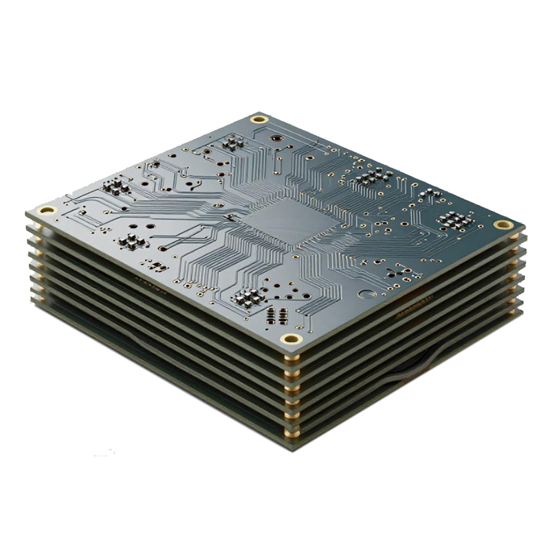
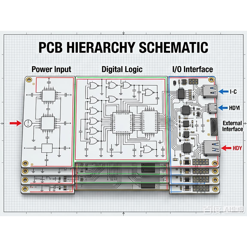
Description
Common Substrates
FR-4, aluminum base PCB, high-frequency substrates including Rogers, Taconic, Arlon and PTFE microwave laminates
Key Electrical & Structural Parameters
Strict tolerance control of step depth to guarantee assembly clearance matching
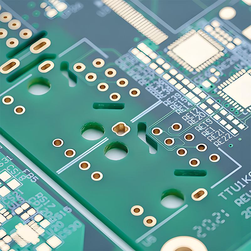
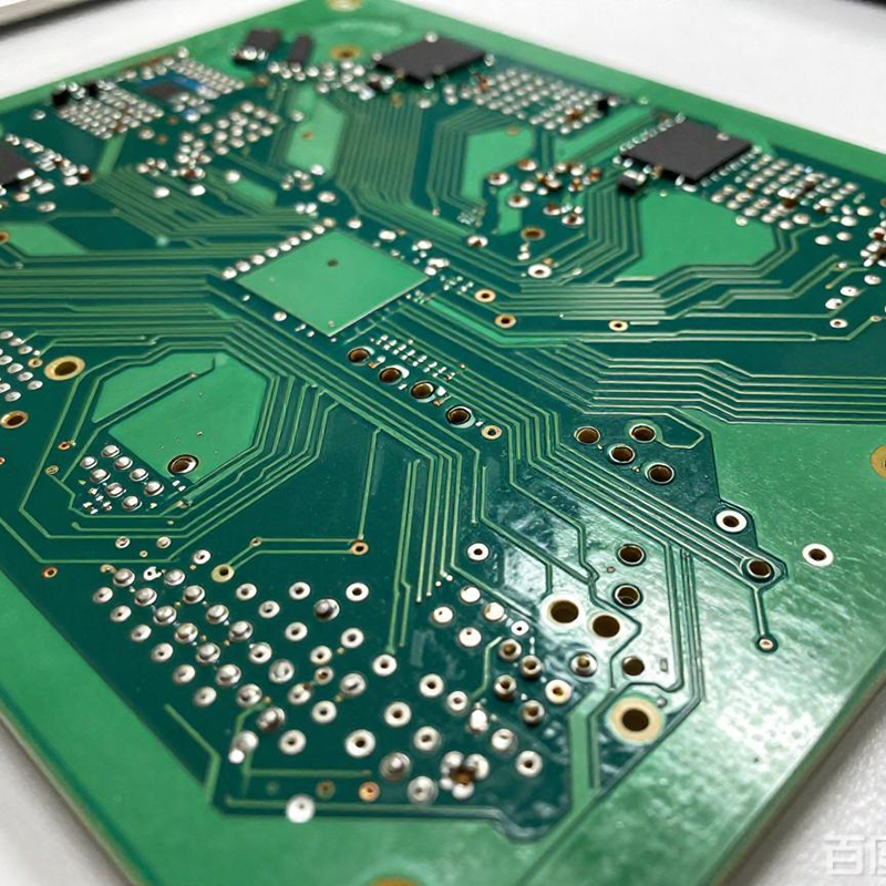
Traces, solder mask openings and components can be arranged on stepped areas
Inner circuit integrity maintained without damage
Support single-sided step, double-sided step and multi-level step design
Manufacturing Challenges & Capabilities
Step routing easily causes substrate chipping and inner copper scratch, requiring special cutters and depth-controlled programs
Layers: 1 ~ 12 layers
Step depth accuracy: ±0.05mm
Gold plating / immersion silver available on stepped zones for reliable soldering
Support combined processes: step PCB + impedance control, step PCB + backdrilling
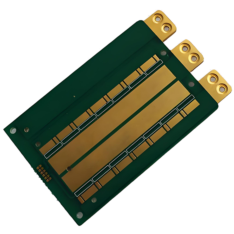
Reviews
There are no reviews yet.