

Description
Common Substrates
Standard FR-4, high Tg FR-4, halogen-free laminates; high-speed materials including Megtron & Isola; high-frequency special substrates such as Rogers, Taconic, Arlon.
Key Electrical Parameters
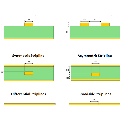
Support single-ended impedance, differential impedance and coplanar waveguide impedance design
Standard impedance tolerance: ±5%; ±3% available for premium RF & high-speed projects
Available impedance range: 25Ω ~ 120Ω (typical: 50Ω, 75Ω, 100Ω differential)
Impedance simulation and production verification strictly carried out according to stack-up documents
Manufacturing Capabilities
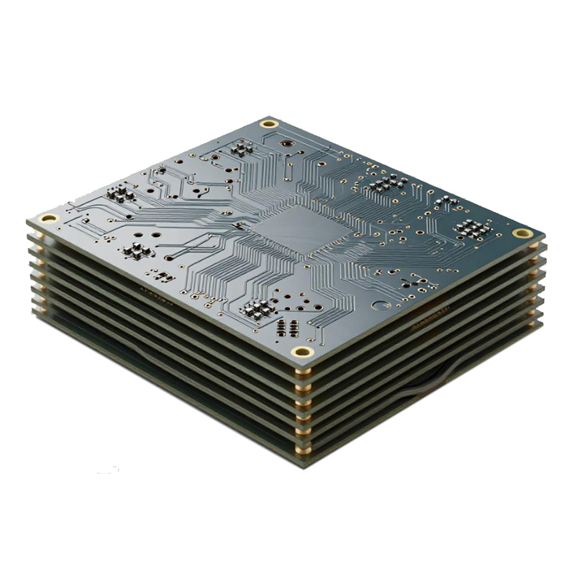
Layers: 2 ~ 24 layers
Minimum trace width / spacing: 3mil / 3mil
Support hybrid stack-up, high-frequency material mixed with FR-4
Surface finishes: ENIG, Immersion Silver, OSP, HASL etc.
Measured impedance test reports available upon request
Reviews
There are no reviews yet.