
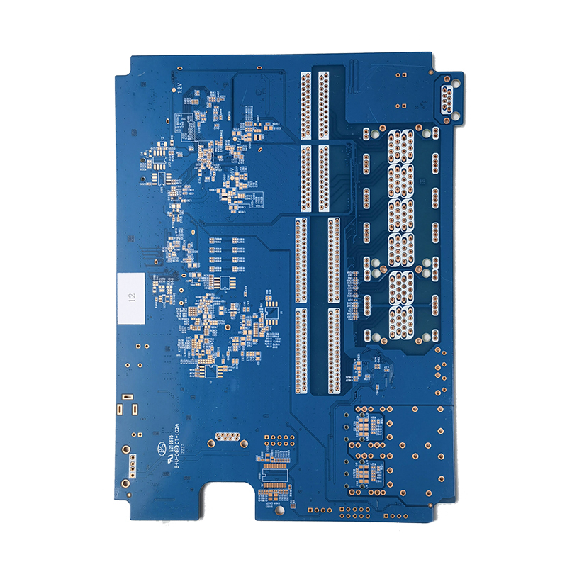
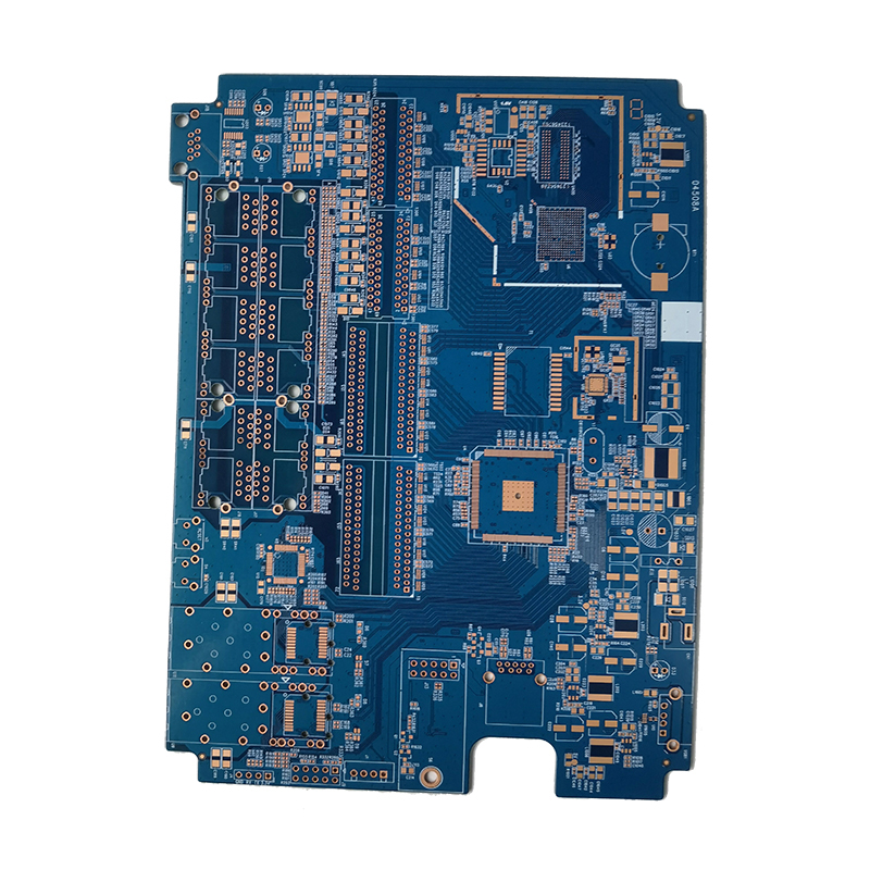
Description
Specifications & Functional Features
– Surface Material: Organic Solderability Preservative Film
– Film Thickness: 0.2–0.5μm (ultra-thin and uniform)
– Surface Flatness: Perfect flatness, zero unevenness
– Environmental Performance: Green, non-toxic, fully RoHS compliant
– Solderability: Excellent, suitable for ultra-fine line and fine-pitch component soldering
– Process Advantage: Lowest cost among all lead-free finishes, super flat, no solder bridging
– Limitations: Short shelf life (3–6 months), only supports limited reflow times, strict vacuum packaging required
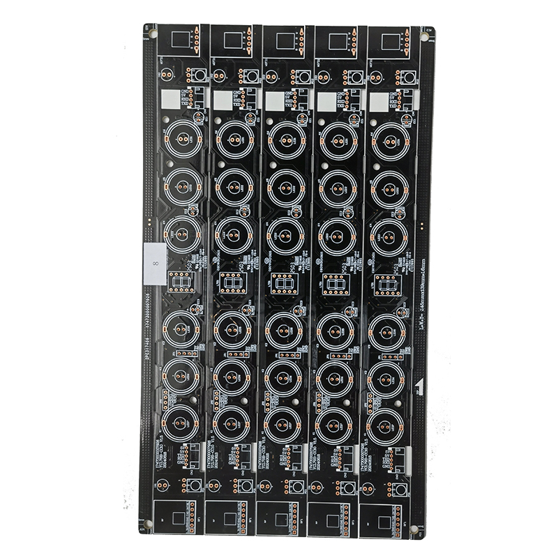
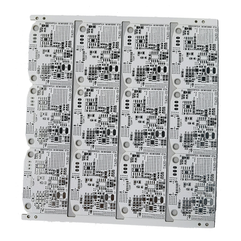
– Typical Applications: Computer motherboards, precision consumer electronics, 5G small signal boards, high-density fine-line PCBs
Working Principle & Process Diagram Description
Working Principle: Organic molecular self-assembly protection. After strict cleaning and micro-etching, the bare copper surface reacts with water-based organic preservative solution (Benzotriazole/Imidazole compounds). Organic molecules form stable coordination bonds with copper atoms, attaching a uniform ultra-thin organic film to cover copper traces. The film isolates oxygen and moisture to prevent oxidation, and it decomposes & volatilizes during high-temperature soldering to expose pure copper for perfect welding.
Process Flow: Acid Cleaning → Micro Etching → Surface Activation → OSP Film Coating → Low-temperature Drying
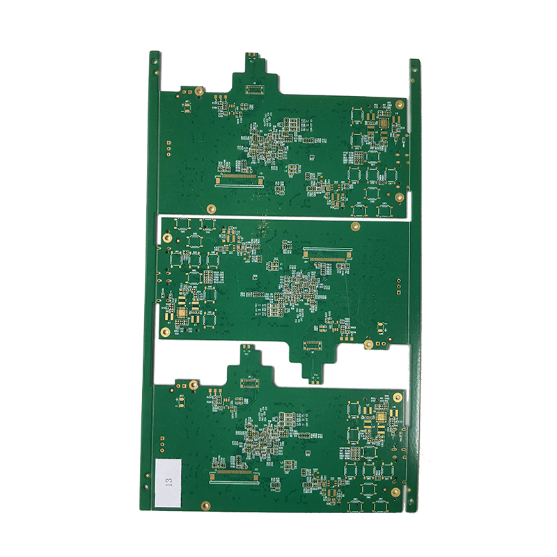
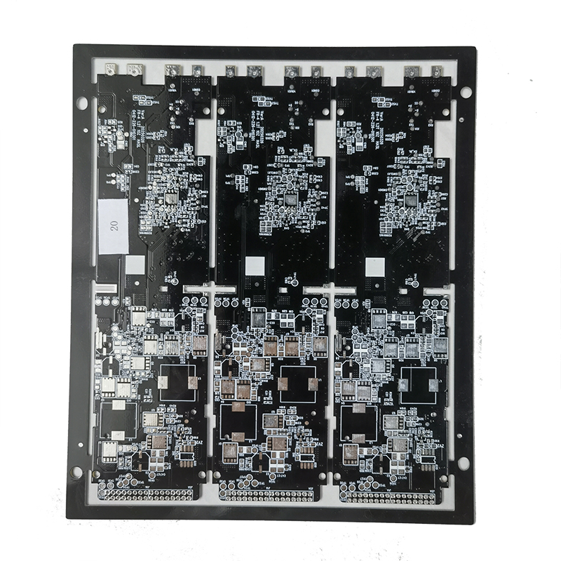
Reviews
There are no reviews yet.