
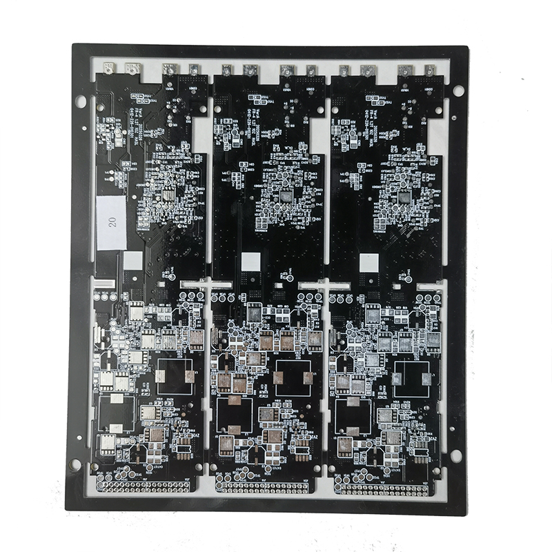
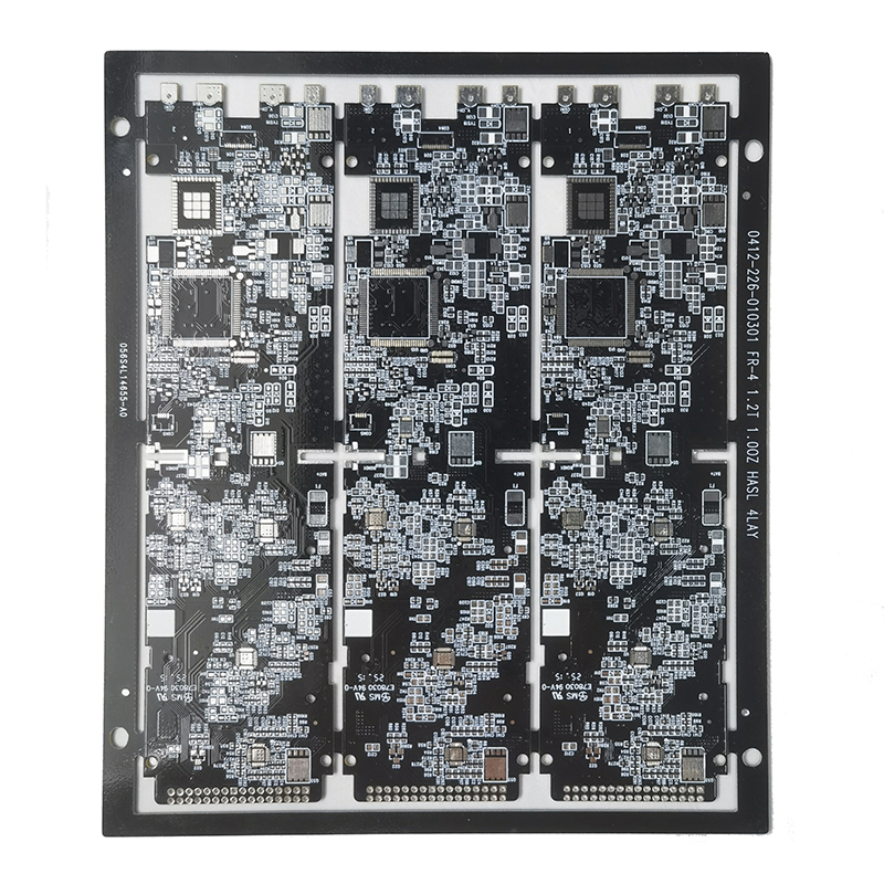
Description
Specifications & Functional Features
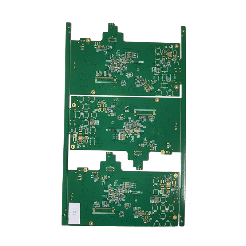
– Surface Material: Tin-Lead Alloy (Sn63/Pb37)
– Coating Thickness: 1.5μm – 3.5μm
– Solderability: Excellent, suitable for wave soldering and reflow soldering
– Oxidation Resistance: Good, long shelf life for ordinary storage environments
– Surface Flatness: Normal, slight uneven surface after hot air leveling
– Process Advantage: Ultra-low cost, high production efficiency, high yield, no strict packaging requirements
– Limitations: Not suitable for fine-pitch components, BGA and QFN; unable to meet lead-free environmental standards
– Typical Applications: Ordinary consumer electronics, power boards, household appliance circuits, industrial control low-end boards
Working Principle & Process Diagram Description
Working Principle: A physical coating & leveling process. The bare copper pads are fully immersed in high-temperature molten tin-lead alloy (Sn63/Pb37). After copper surface adsorbs solder alloy, high-pressure hot air blows off excess solder and levels the pad surface to form a uniform thick tin-lead protective layer, isolating copper from air oxidation.
Process Flow: Board Cleaning → Flux Coating → Molten Solder Dipping → Hot Air Leveling → Cooling & Inspection
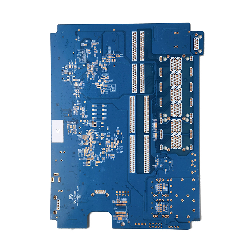
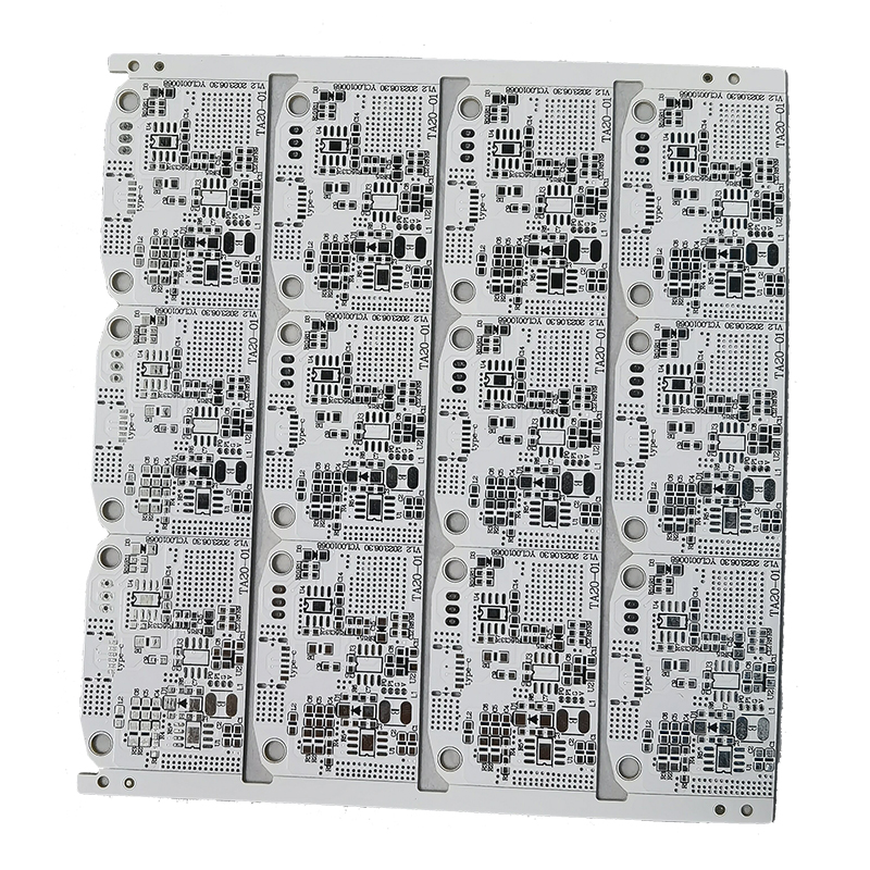
Reviews
There are no reviews yet.