
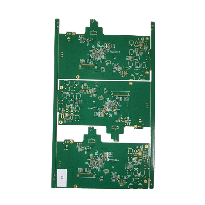
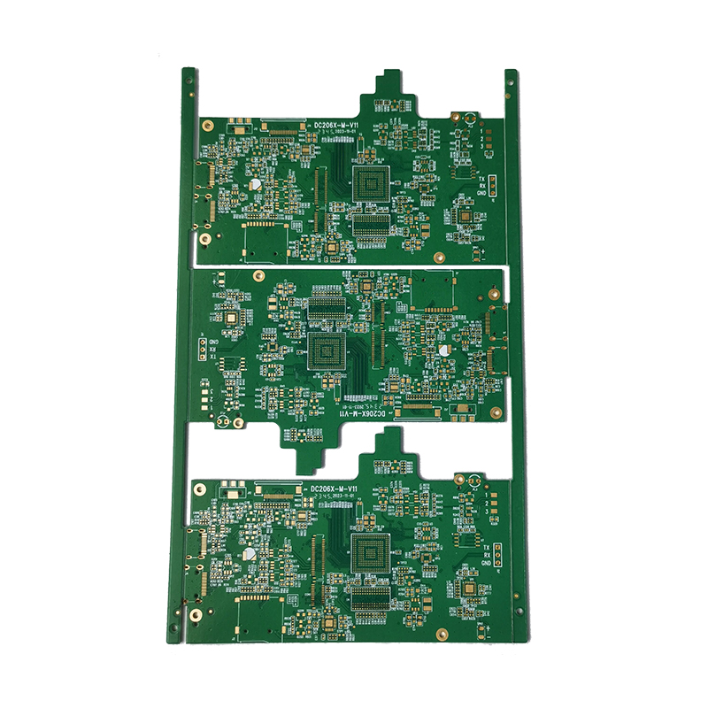
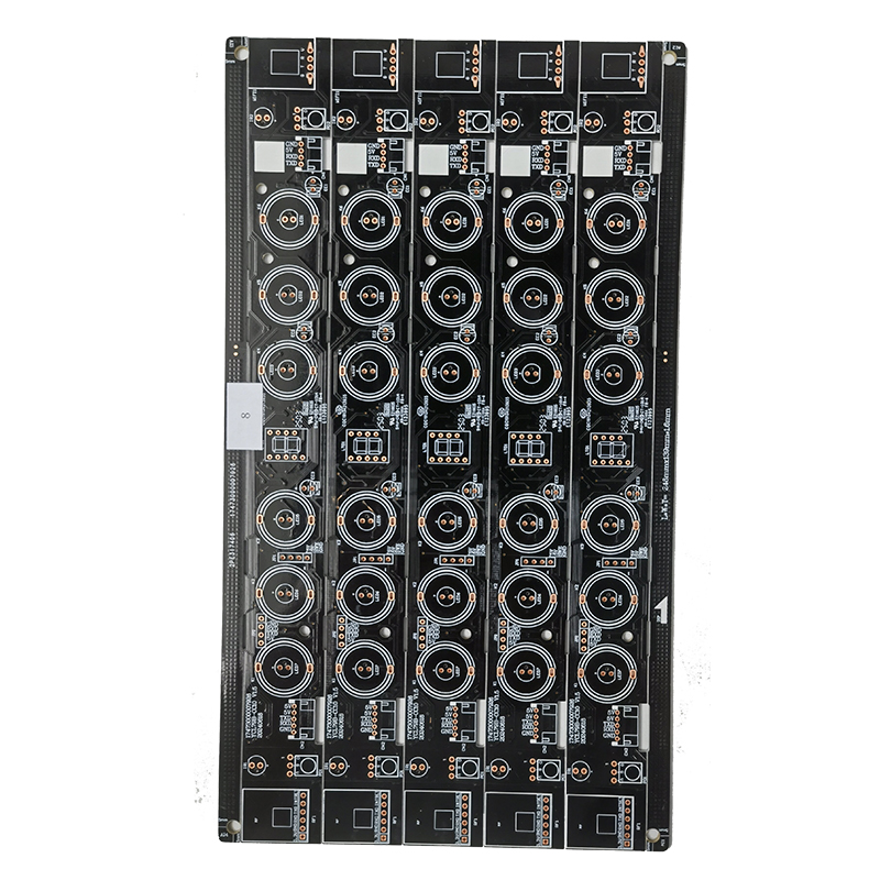
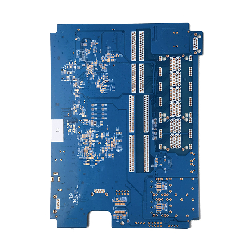
Description
Specifications & Functional Features
– Structure: Electroplated Nickel Underlayer + Electroplated Hard Gold Layer
– Layer Thickness: Nickel 3.0–8.0μm, Hard Gold 0.3–3.0μm (customizable)
– Hardness & Wear Resistance: Ultra-high hardness, resistant to repeated friction and plug-in wear
– Oxidation & Corrosion Resistance: Excellent, suitable for long-term use in harsh environments
– Conductivity: Super stable, no contact resistance change after long-term use
– Process Advantage: Customizable gold thickness, extreme durability, reliable contact performance
– Limitations: High cost, not recommended for fine-pitch soldering mounting
– Typical Applications: Connector contact pins, key switch boards, Bluetooth antenna contacts, industrial equipment conductive terminals, wearable device contact boards
Working Principle & Process Diagram Description
Working Principle: Current-assisted electroplating deposition. With external DC power supply, nickel ions are electroplated onto cleaned copper pads to form a thick nickel base layer. Then hard gold solution is used, and gold alloy ions are uniformly deposited on the nickel layer under current action to form a high-hardness, thick hard gold coating. The metallic layered structure provides ultra wear resistance and stable contact conductivity.
Process Flow: Precision Cleaning → Electrolytic Degreasing → Electroplated Nickel Bottom → Electroplated Hard Gold → Post-treatment & Drying
Reviews
There are no reviews yet.