Description
Specifications & Functional Features
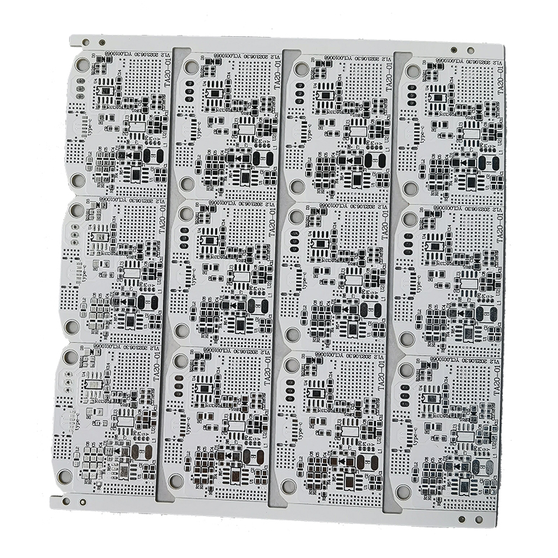
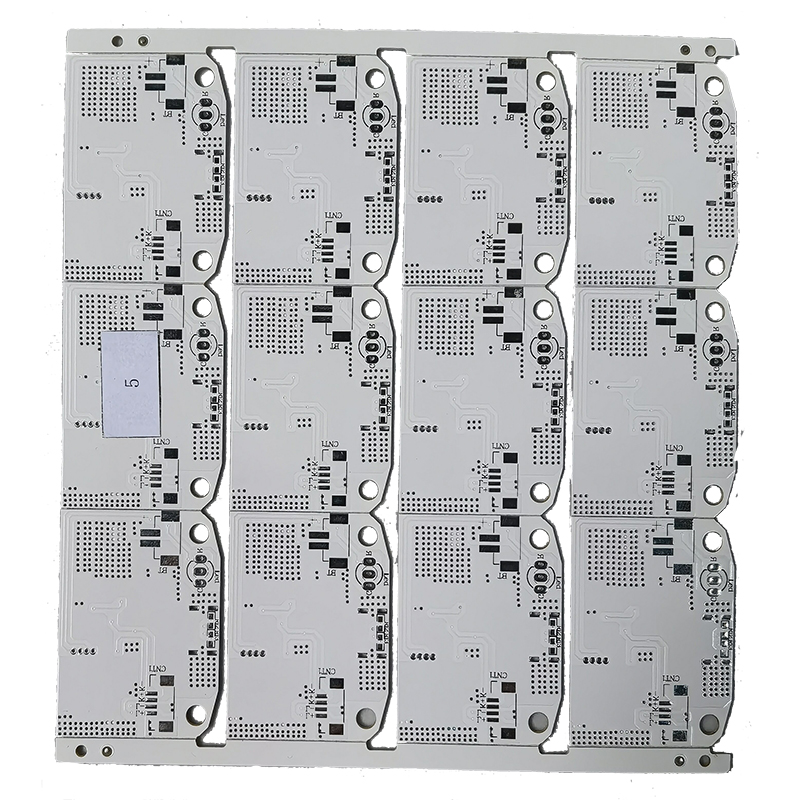
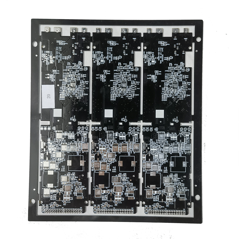
– Surface Material: Pure Tin (Lead-Free)
– Coating Thickness: 1.2μm – 3.0μm
– Compliance: Fully RoHS & REACH compliant
– Solderability: Good, stable performance for multiple reflow soldering
– Surface Flatness: Moderate, better than traditional leaded HASL
– Process Advantage: Cost-efficient, environmentally friendly, high production speed, strong applicability for mass orders
– Limitations: Not applicable for ultra-fine line width and high-precision BGA packaging
– Typical Applications: Mass consumer electronics, automotive ordinary circuits, industrial control equipment, communication basic boards
Working Principle & Process Diagram Description
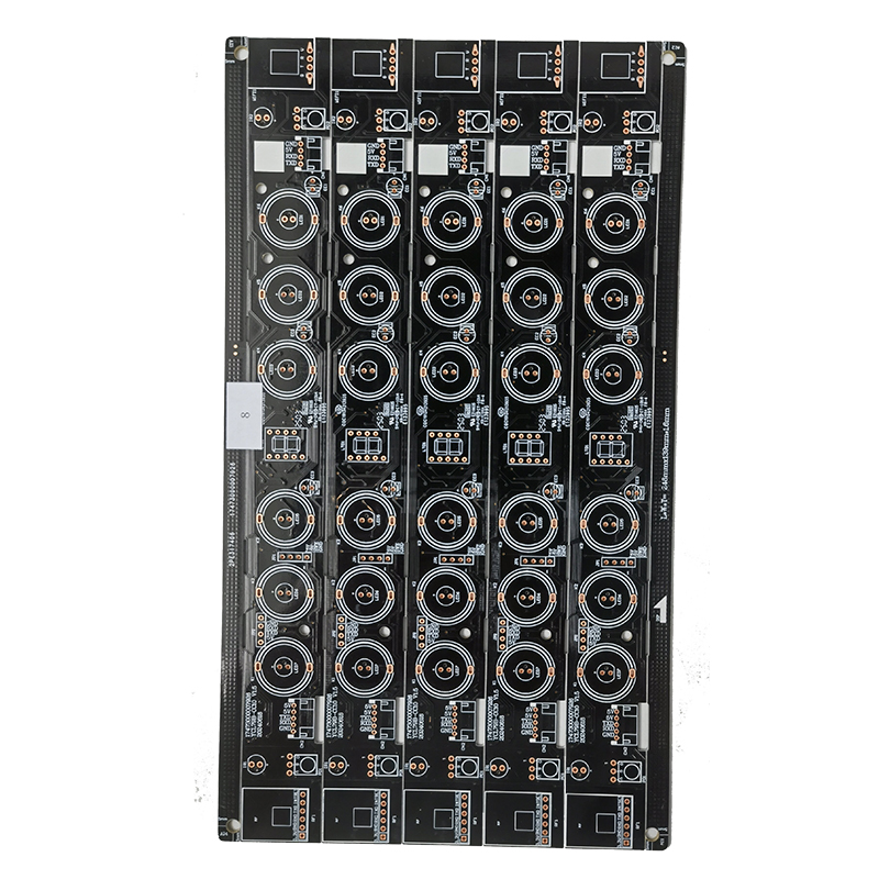
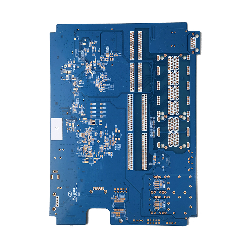
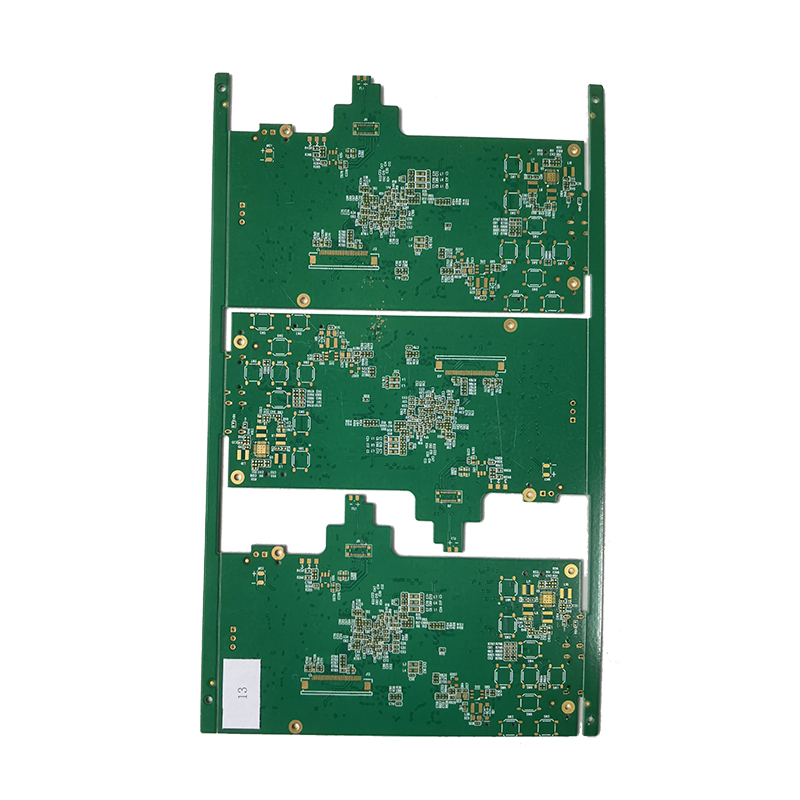
Working Principle: Eco-friendly physical hot air leveling process. Replace tin-lead alloy with high-purity molten pure tin. The cleaned copper pads absorb pure tin solder, then hot air trimming removes redundant tin to form a dense pure tin protective layer on copper surface, achieving anti-oxidation and lead-free soldering performance.
Process Flow: Acid Cleaning → Micro Etching → Flux Application → Lead-Free Pure Tin Dipping → Hot Air Leveling → Drying & Quality Check
Reviews
There are no reviews yet.