
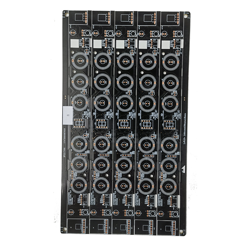
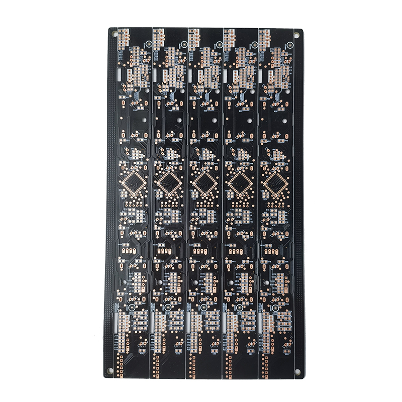
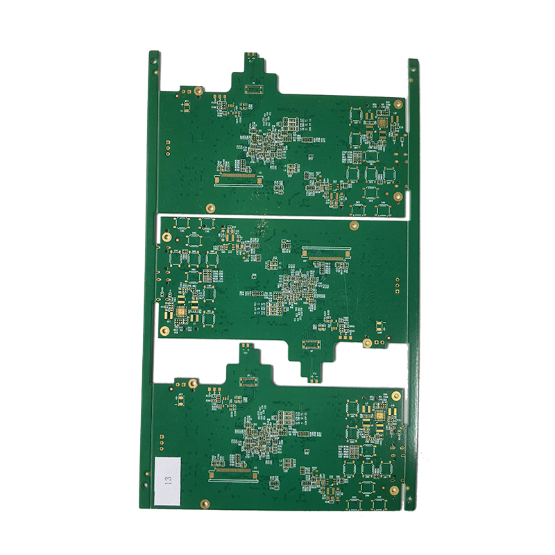
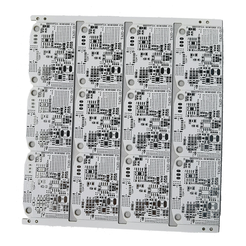
Description
Specifications & Functional Features
– Structure: Electroless Nickel Layer + Immersion Gold Layer
– Layer Thickness: Nickel 2.0–5.0μm, Gold 0.05–0.12μm
– Surface Flatness: Excellent, completely flat for fine-pitch mounting
– Oxidation Resistance: Super strong, shelf life up to 12 months under standard storage
– Solderability: Perfect, supports multiple reflow soldering
– Conductivity: Stable, ideal for signal transmission modules
– Process Advantage: No solder bridge for fine lines, high bonding strength, high reliability
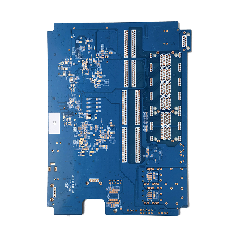
– Typical Applications: BGA/QFN packaging boards, communication modules, medical electronics, automotive high-precision circuits, smart device motherboards
Working Principle & Process Diagram Description
Working Principle: Dual-layer chemical redox reaction deposition, no electricity required. Step 1: Activated copper surface induces autocatalytic reaction to deposit dense Nickel-Phosphorus (Ni-P) alloy layer, serving as barrier layer to block copper diffusion. Step 2: Gold ions replace nickel atoms via displacement reaction, forming an ultra-thin pure gold layer on nickel surface. Double-layer structure ensures flatness, solderability and long-term anti-oxidation.
Process Flow: Degreasing & Cleaning → Micro Etching → Surface Activation → Electroless Nickel Deposition → Immersion Gold Displacement → Drying
Reviews
There are no reviews yet.