
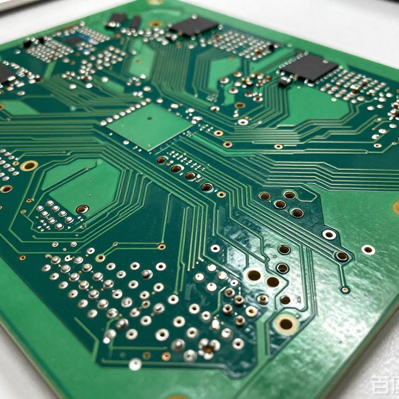

Description
Common Substrates
High-speed FR-4, Megtron, Isola series; high-frequency substrates such as Rogers, Arlon, Taconic
Key Electrical Parameters
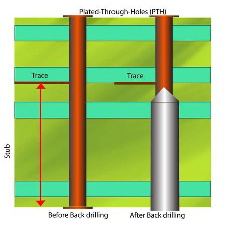
Minimize via stub length and suppress high-frequency resonance
Optimize return loss and insertion loss performance
Ensure stable transmission for 10Gbps ~ 112Gbps high-speed SerDes links
Reduce inter-channel crosstalk
Manufacturing Challenges & Capabilities
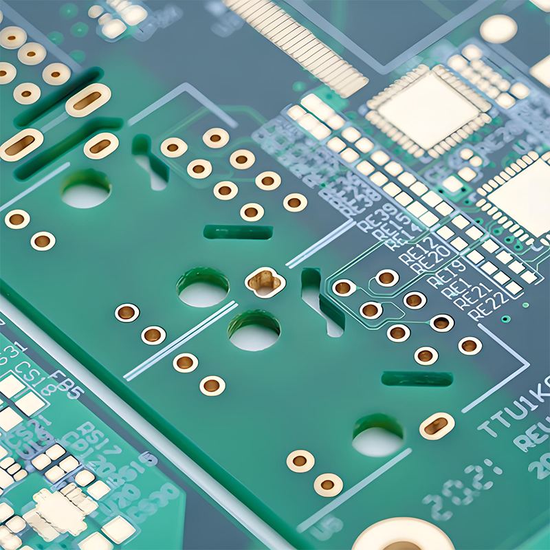
Extremely high precision required for backdrill depth to avoid damage to functional inner traces
Layers: 4 ~ 24 layers, optimized for thick backplanes
Remaining stub length can be controlled ≤5mil
Backdrill depth tolerance: ±0.025mm
Support combined processes: backdrilling + impedance control, backdrilling + blind & buried vias
General Application Fields
Communication base stations, server backplanes, high-speed switches, optical communication modules, new energy power supplies, energy storage inverters, RF cavity modules, industrial control systems, millimeter-wave radars, test & measurement instruments, aerospace electronics.
Reviews
There are no reviews yet.