
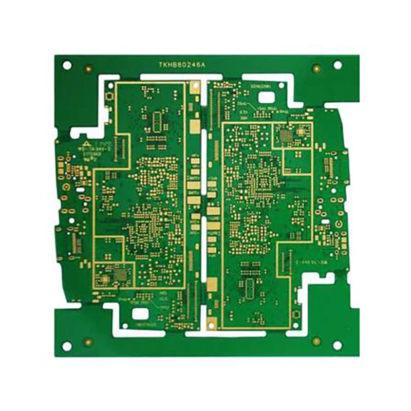

Description
Micro Ultra-small Aperture: Minimum laser blind hole diameter up to 3mil (75μm), extreme precision up to 2mil (50μm)
Standard Aspect Ratio: Optimized blind hole aspect ratio ≤1:1, ensuring uniform electroplating and stable hole conduction
Diversified Hole Processing: Supports resin plug hole and copper-filled hole processes, compatible with stacked and staggered microvia structures
High-precision Alignment: Adopts RCC resin-coated copper foil material, with precise lamination and desmear process to eliminate hidden dangers of poor hole conductivity
Applications
Smart wearable devices, mobile phone precision modules, camera PCBs, 5G mini communication units, automotive precision electronic boards

Reviews
There are no reviews yet.