


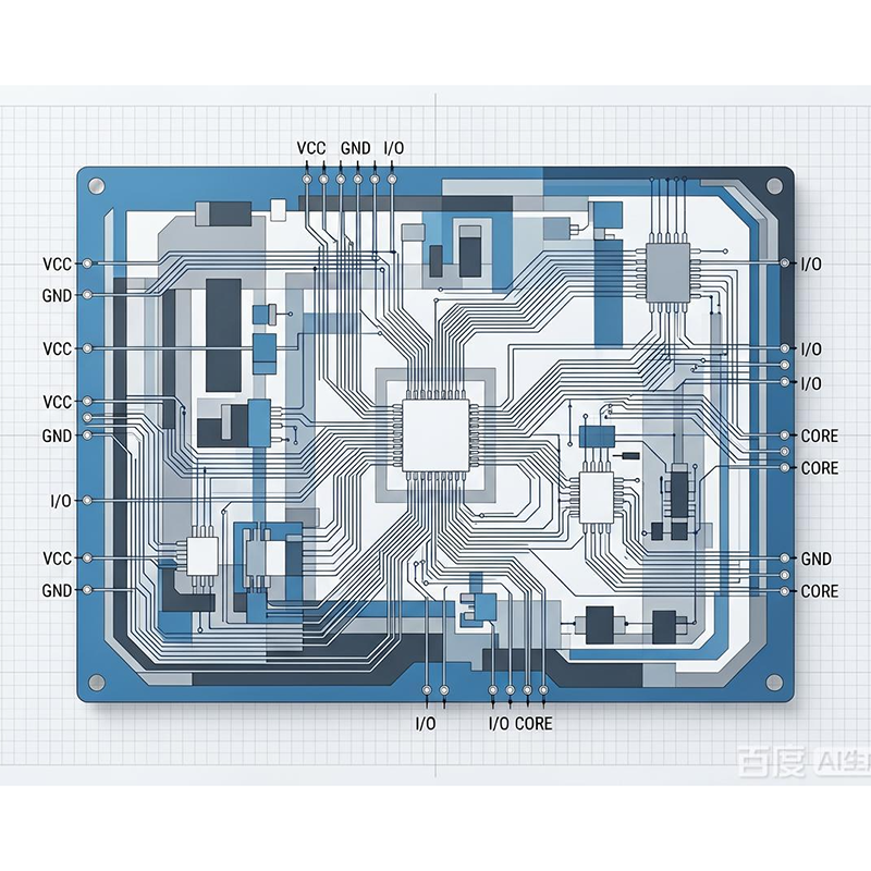
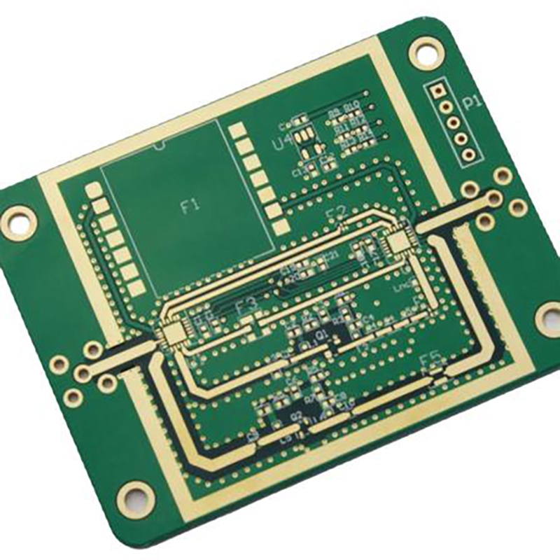
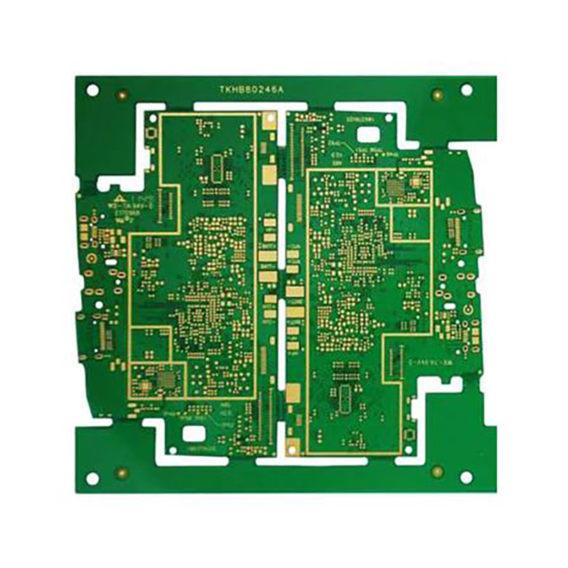
Description
Ultra-fine Routing Capability: Minimum line width/line space up to 2mil/2mil (50μm/50μm), extreme precision up to 1.5mil/1.5mil
High-precision Process: Adopts low-profile thin copper foil (1/4oz, 1/3oz, 1/2oz) to avoid side etching and ensure complete and smooth circuit traces
High Reliability: Matches high-Tg substrate with stable physical properties, effectively preventing circuit open/short defects
Wide Adaptability: Supports 2–24 layers of multi-layer boards, suitable for high-density inner-layer routing of HDI boards and high-precision module boards
Reviews
There are no reviews yet.