Description
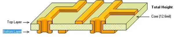

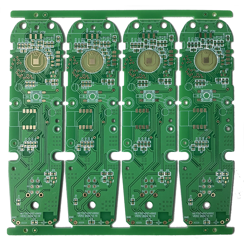
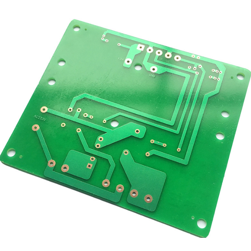
Circuit traces exist on both top and bottom surfaces. Metallized vias electrically connect the two copper layers, greatly improving layout freedom without jump wires. Widely used for medium-complex electronic products.
| Item | Double-sided PCB(Double Layer PCB) |
|---|---|
| Conductive Layers | Copper traces on both top& bottom sides |
| Via Structure | Metallized through viasconnect top & bottomlayers |
| Wiring Density | Medium. Higher layoutflexibility |
| Cost Level | Moderate |
| Manufacturing Cycle | Medium |
| Electrical Performance | Acceptable for generalcircuitsLimited EMI suppression |
| Typical Applications | Sensors, industrial controlmodules, audio equipment,general consumerelectronics |
| Main Limitation | No inner layers; insufficientfor complex high-speedcircuits |
Reviews
There are no reviews yet.