

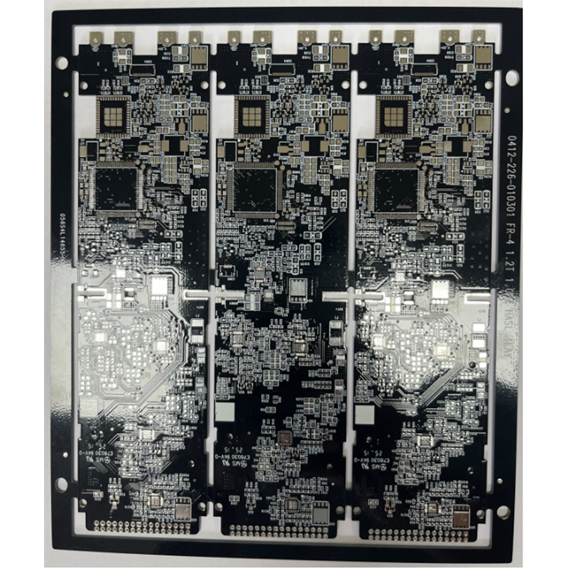
This product is a 4-layer printed circuit board (PCB) with tin-sprayed surface finish and metal edge wrapping technology, designed for applications requiring enhanced shielding performance, stable electrical connectivity, and reliable solderability. The 4-layer stack-up ensures efficient signal routing, while the tin spraying and metal edge wrapping improve durability and electromagnetic compatibility (EMC).
4-layer multilayer structure: Supports stable power distribution and complex circuit routing
Tin-sprayed surface finish: Provides excellent solderability and anti-oxidation protection
Metal edge wrapping design: Enhances shielding, grounding continuity, and mechanical strength
Improved EMC performance: Reduces electromagnetic interference (EMI) in high-frequency environments
Strong structural reliability: Reinforced edges improve durability during assembly and operation
Cost-effective shielding solution: Combines performance and manufacturability
Layer count: 4 layers
Base material: FR-4 / high-Tg FR-4 (optional)
Surface finish: Tin spraying (Sn coating)
Edge treatment: Metal edge wrapping (conductive plating or shielding wrap)
Tin thickness: 5–30 μm (customizable)
Copper thickness: 1 oz / 2 oz (customizable)
Board thickness: 0.8 mm – 2.4 mm
Minimum trace/space: 4/4 mil (depending on design capability)
Operating temperature: -40°C to 130°C (standard FR-4)
Communication equipment and RF modules
Industrial control systems
Automotive electronic control units (ECUs)
Power supply systems
High-speed digital circuits
EMI-sensitive electronic devices
Embedded control boards
Compared with standard 4-layer tin-sprayed PCBs, this metal edge wrapped design provides:
Better electromagnetic shielding and signal integrity
Improved grounding performance across board edges
Enhanced mechanical robustness during assembly and vibration
Reduced EMI leakage in high-frequency applications
Longer service life in harsh operating environments
Edge wrapping method (full wrap / partial / selective grounding)
Tin thickness adjustment
Base material selection (FR-4, high-Tg FR-4)
Stack-up design optimization
Copper weight and impedance control
Solder mask color options (green, black, blue, red, white)
Each PCB is manufactured under strict quality control processes, including:
Electrical testing (E-test)
AOI (Automated Optical Inspection)
Impedance and continuity verification
Edge plating adhesion testing
Solderability testing
Dimensional and structural inspection